LED junction temperature, what is the LED junction temperature, what causes the LED junction temperature, and what are the ways to reduce the LED junction temperature? The following will analyze in detail 1. What is the junction temperature of the High power LED? The basic structure of High power LED is a semiconductor P-N junction. The experiment pointed out that when current flows through the LED element, the temperature of the P-N junction will rise. Strictly speaking, the temperature of the P-N junction area is defined as the junction temperature of the LED. Usually because the component chips have a small size, we can also regard the temperature of the LED chip as the junction temperature.
2. What are the reasons for the LED junction temperature? When the HIGH POWER LED is working, there can be the following five conditions to cause the junction temperature to rise to different degrees: Value, these resistances add to each other to form the series resistance of the LED element. When current flows through the P-N junction, it will also flow through these resistors, thereby generating Joule heat, causing the chip temperature or junction temperature to rise.
b, b. Since the PN junction cannot be extremely perfect, the injection efficiency of the component will not reach 100%. Charges (electrons) will also be injected into the P area. Generally, the latter type of charge injection will not produce a photoelectric effect, but will be consumed in the form of heat. Even if the useful part of the injected charge, it will not all become light, and some of it will become heat when combined with impurities or defects in the junction area. c, c. Practice has proved that the limitation of light extraction efficiency is the main reason for the increase of High power LED junction temperature. At present, advanced material growth and component manufacturing processes can convert most of the input electrical energy of the LED into light radiation energy. However, compared with the surrounding medium, the LED chip material has a much larger refractive index, resulting in the internal generation of the chip. A large part of the photons (>90%) cannot smoothly overflow the interface, and total reflection occurs at the interface between the chip and the medium, returns to the inside of the chip and is finally absorbed by the chip material or substrate through multiple internal reflections, and is in the form of lattice vibration Becomes hot, causing the junction temperature to rise. d, d. Obviously, the heat dissipation capacity of HIGH POWER LED components is another key condition that determines the junction temperature. When the heat dissipation capacity is strong, the junction temperature will decrease, and conversely, when the heat dissipation capacity is poor, the junction temperature will increase. Since epoxy glue is a low thermal conductivity material, it is difficult for the heat generated at the PN junction to be radiated upwards to the environment through the transparent epoxy. Most of the heat passes through the substrate, silver paste, shell, epoxy adhesive layer, PCB and The heat sink diverges downward. Obviously, the thermal conductivity of related materials will directly affect the heat dissipation efficiency of the component. An ordinary HIGH POWER LED, the total thermal resistance from the PN junction area to the ambient temperature is between 300 and 600°C/w. For a power LED component with a good structure, the total thermal resistance is about 15 to 30°C/w The huge difference in thermal resistance indicates that ordinary HIGH POWER LED components can only work normally under a small input power condition, while the dissipation power of power components can be as large as watts or even higher. 3. What are the ways to reduce the HIGH POWER LED junction temperature? Mad The input power of the component is the only source of the thermal effect of the component. Part of the energy becomes radiant light energy, and part of it eventually becomes heat, which raises the temperature of the component. Obviously, the main method to reduce the LED temperature rise effect is to try to improve the electro-optical conversion efficiency (also known as external quantum efficiency) of the element, so that as much input power as possible is converted into light energy, and another important way is to try to improve the element The heat dissipation capacity of the heat dissipation capacity enables the heat generated by the junction temperature to be dissipated to the surrounding environment through various channels.
Led is afraid of high temperature. Its junction temperature is 125 degrees. The maximum withstand temperature of HIGH POWER LED is 80 degrees. The temperature of the whole lamp shell is generally less than 65 degrees. The lower the temperature, the better. The high-power temperature is generally 80 degrees. Normally, when the heat dissipation is not ideal and the junction temperature rises during operation, the voltage will increase slightly, causing the current to increase, and even burn the internal gold wire. The solution is to use a constant current source to drive the LED. The shape of the LED is epoxy glue. It is not uncommon for the air temperature to cause a dead light, but it should not exceed 200 degrees. If the light is not on, the static electricity may cause leakage of the light-emitting chip inside, and then the light will die. There is also the temperature requirement during operation. Because HIGH POWER LEDs are generally used by welding, the welding position is at least 3MM soldering iron under the LED gel. The maximum temperature is 260 degrees and the longest time is 3S, but this is only a requirement in the specification when using normal LEDs. Sometimes the lamp may not be dead if it exceeds this requirement, but it must be normal to use LED within this requirement, as long as the anti-static is in place during operation. HIGH POWER LED is a photoelectric device. During its working process, only 15%-25% of the electric energy is converted into light energy, and the rest of the electric energy is almost converted into heat energy, which increases the temperature of the HIGH POWER LED. In high-power LEDs, heat dissipation is a big problem. For example, if a 10W white LED has a photoelectric conversion efficiency of 20%, 8W of electrical energy is converted into heat. If no heat dissipation measures are taken, the core temperature of the high-power LED will rise rapidly, when its junction temperature (TJ) When the temperature rises above the maximum allowable temperature (usually 150°C), the high-power LED will be damaged due to overheating. Therefore, in the design of high-power LED lamps, the most important design work is heat dissipation design. Otto However, in the heat dissipation design of high-power LEDs, the junction temperature TJ requirement is much lower than 125°C. The reason is that TJ has a greater impact on the light extraction rate and life of the LED: the higher the TJ, the lower the light extraction rate and the shorter the life of the LED. The relationship between the junction temperature TJ of K2 series white HIGH POWER LEDs and the relative light output rate. When TJ=25℃, the relative light output rate is 1; when TJ=70℃, the relative light output rate drops to 0.9; when TJ=115℃, it drops to 0.8. When TJ=50℃, the service life is 90000 hours; when TJ=80℃, the service life is reduced to 34000 hours; when TJ=115℃, its service life is only 13,300 hours. TJ should put forward the maximum allowable junction temperature value TJmax in the heat dissipation design, and the actual junction temperature value TJ should be less than or equal to the required TJmax, that is, TJ≤TJmax.
The heat dissipation path of high-power LEDs. High-power LEDs attach great importance to heat dissipation in structural design. Figure 2 is the internal structure of Lumiled's K2 series, and Figure 3 is the internal structure of NCCW022 of NICHIA. It can be seen from these two figures that there is a large-sized metal heat dissipation pad under the die, which can transfer the heat of the die to the outside through the heat dissipation pad. The high-power LED is soldered on the printed circuit board (PCB), as shown in Figure 4. The bottom surface of the heat dissipation pad is welded to the copper-clad surface of the PCB, and a larger copper-clad layer is used as the heat dissipation surface. In order to improve the heat dissipation efficiency, a double-layer copper-clad PCB is used, and the front and back graphics are shown in Figure 5. This is the simplest heat dissipation structure. Heat is dissipated from a high temperature place to a low temperature place. The main heat dissipation path of high-power LED is: die→heat dissipation pad→copper layer of printed board→printed board→ambient air. If the junction temperature of the LED is TJ, the temperature of the ambient air is TA, and the temperature at the bottom of the heat sink is Tc (TJ>Tc>TA), the heat dissipation path is shown in Figure 6. In the process of heat conduction, the thermal conductivity of various materials is different, that is, there are different thermal resistances. If the thermal resistance of the die conducted to the bottom surface of the heat sink is RJC (thermal resistance of the LED), the thermal resistance of the heat sink to the copper layer of the PCB surface layer is RCB, and the thermal resistance of the PCB to the ambient air is RBA, then the thermal resistance from the tube The relationship between the total thermal resistance RJA of the core junction temperature TJ conducted to the air TA and each thermal resistance is: RJA=RJC+RCB+RBA The unit of each thermal resistance is ℃/W.
It can be understood like this: the smaller the thermal resistance, the better the thermal conductivity, that is, the better the heat dissipation performance. If the heat sink pad of the High power LED and the copper layer of the PCB are soldered together by reflow soldering, then RCB=0, the above formula can be written as: RJA=RJC+RBA The calculation formula for heat dissipation If the junction temperature is TJ, the ambient temperature is TA, LED The power consumption is PD, then the relationship between RJA and TJ, TA and PD is: RJA=(TJ-TA)/PD (1) where the unit of PD is W. The relationship between the forward voltage drop VF of the PD and the LED and the forward current IF of the LED is: PD=VF×IF (2) If the temperature TC of the LED cooling pad has been measured, the formula (1) can be written as: RJA=( TJ-TC)/PD+(TC-TA)/PD then RJC=(TJ-TC)/PD (3) RBA=(TC-TC)/PD (4) In the heat dissipation calculation, when the high-power LED is selected , The RJC value can be found from the data; when the forward current IF of the LED is determined, the PD can be calculated according to the VF of the LED; if the temperature of the TC has been measured, the TJ can be calculated according to the formula (3). Before measuring TC, make an experiment board (choose a certain kind of PCB, determine a certain area), solder the High power LED, input the IF current, and wait for stability, then use a K-type thermocouple point thermometer to measure the temperature TC of the LED's cooling pad. In equation (4), TC and TA can be measured, PD can be calculated, and the RBA value can be calculated. If TJ is calculated, RJA can be obtained by substituting equation (1). This method of calculating TJ through experiments is based on the use of a certain PCB and a certain heat dissipation area. If the calculated TJ is less than the required (or equal to) TJmax, the selected PCB and area can be considered appropriate; if the calculated TJ is greater than the required TJmax, a PCB with better heat dissipation performance should be replaced, or the heat dissipation area of the PCB should be increased. In addition, if the RJC value of the selected LED is too large, the high-power LED with better performance and smaller RJC value can also be replaced in the design to satisfy the calculated TJ≤TJmax. This is illustrated in the calculation example.
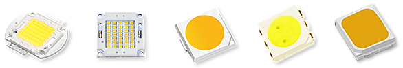
Various PCBs At present, there are three types of PCBs used with high-power LEDs for heat dissipation: ordinary double-sided copper-clad boards (FR4), aluminum alloy-based copper-clad boards (MCPCB), and flexible film PCBs glued to aluminum alloy boards. The structure of MCPCB is shown as in Fig. 7. The thickness dimensions of each layer are shown in Table 3. The heat dissipation effect is related to the thickness of the copper layer and the metal layer and the thermal conductivity of the insulating medium. MCPCB with 35μm copper layer and 1.5mm aluminum alloy is generally used. The structure of the flexible PCB glued on the aluminum alloy board is shown in Figure 8. The thickness dimensions of each layer generally used are shown in Table 4. 1~3W star-shaped LED adopts this structure. MCPCB with high thermal conductivity medium has the best heat dissipation performance, but the price is more expensive. Calculation example Here we take part of the data from NICHIA's TC measurement example as a calculation example. The known conditions are as follows: LED: 3W white LED, model MCCW022, RJC=16℃/W. The measuring head of the K-type thermocouple point thermometer is welded on the heat dissipation pad. PCB test board: double-layer copper-clad board (40×40mm), t=1.6mm, copper layer area on the welding surface 1180mm2, copper layer area on the back side is 1600mm2. LED working status: IF=500mA, VF=3.97V. Measure TC with K-type thermocouple point thermometer, TC=71℃. Ambient temperature TA = 25℃ during testing. 1. TJ calculation TJ=RJC×PD+TC=RJC(IF×VF)+TC TJ=16℃/W(500mA×3.97V) +71℃=103℃ 2.RBA Calculate RJA=(TC-TA)/PD=(71℃-25℃)/1.99W=23.1℃/W 3. Calculate RJA RJA=RJC+RBA =16℃/W+23.1℃/W =39.1℃/W If the designed TJmax=90℃, the TJ calculated according to the above conditions cannot meet the design requirements. It is necessary to change the PCB with better heat dissipation or increase the heat dissipation area, and test and calculate again until TJ≤TJmax is met. Another method is that when the RJC value of the LED used is too large, if a new type of similar product is replaced with RJC=9°C/W (VF=3.65V when IF=500mA), and other conditions remain unchanged, TJ is calculated as: TJ= 9℃/W(500mA×3.65V)+71℃=87.4℃ There are some errors in 71℃ in the above formula. We should solder a new 9℃/W LED and re-test TC (the measured value is slightly smaller than 71℃ ). This has little effect on calculations. After adopting 9℃/W LED, there is no need to change PCB material and area, and its TJ meets the design requirements. If the calculated TJ with a heat sink on the back of the PCB is much larger than the TJmax required by the design, and the structure does not allow to increase the area, consider sticking the back of the PCB to the "∪"-shaped aluminum profile (or aluminum stamping上), or glued to the heat sink, as shown in Figure 10. These two methods are commonly used in the design of multiple high-power LED lamps. For example, in the above calculation example, a 10°C/W heat sink is pasted on the back of the PCB with TJ=103°C, and its TJ drops to about 80°C. It should be noted that the above TC is measured at room temperature (room temperature is generally 15-30°C). If the ambient temperature TA of the LED lamp is greater than room temperature, the actual TJ will be higher than the TJ calculated after the room temperature measurement, so this factor should be considered in the design. If the test is carried out in a thermostat, the temperature is adjusted to the highest ambient temperature during use, which is the best. In addition, whether the PCB is installed horizontally or vertically, the heat dissipation conditions are different, which has a certain impact on the measurement of TC. The housing material, size and the presence or absence of heat dissipation holes of the lamp also have an impact on the heat dissipation. Therefore, leave room for design. The lower the temperature, the longer the life of the HIGH POWER LED. When doing comparative tests, be sure to install the same heat-dissipating profile for different HIGH POWER LEDs. The chips produced by different manufacturers are mainly due to process problems. Generally, it is better to control the temperature of the chip below 100 degrees. If it is higher, the LED light attenuation is particularly large, but the temperature of the chip cannot be measured. Generally, the heat from the LED chip to the aluminum substrate Caused by hindrance
The temperature difference is about 20 degrees (1W), and the temperature of the aluminum substrate can be measured. We generally control the temperature of the LED aluminum substrate below 60 degrees. The temperature of the wafer is around 80 degrees. The life of the LED SMD 1W is in the laboratory, and the normal temperature is 25 degrees Celsius, and the current is kept within the determined 350MA, and the power harmonics are kept within a very small amount, theoretically. The upper life span will be 50,000 to 100,000 hours. When the lamp bead is working, the temperature of the heat sink should generally be kept not higher than 60 degrees Celsius. The light-emitting wavelength of the HIGH POWER LED changes with the temperature to 0.2-0. 3nm/°C, and the spectral width increases accordingly, which affects the vividness of the color. In addition, when the forward current flows through the pn junction, the heat loss will cause the junction temperature to rise. At around room temperature, for every 1°C increase in temperature, the luminous intensity of the HIGH POWER LED will correspondingly decrease by about 1%, and the package will dissipate heat; Purity and luminous intensity are very important. In the past, the method of reducing its drive current was used to lower the junction temperature. The drive current of most LEDs is limited to about 20mA. However, the light output of the LED will increase with the increase of current. At present, the driving current of many power LEDs can reach 70mA, 100mA or even 1A. It is necessary to improve the packaging structure, a new LED packaging design concept and a low thermal resistance packaging structure and Technology to improve thermal characteristics. For example, a large-area chip flip-chip structure is adopted, silver glue with good thermal conductivity is selected, the surface area of the metal bracket is increased, and the silicon carrier of the solder bump is directly mounted on the heat sink. In addition, in the application design, the thermal design and thermal conductivity of PCB circuit boards are also very important. After entering the 21st century, the high efficiency, ultra-high brightness, and full color of HIGH POWER LED have been continuously developed and innovated. The luminous efficiency of red and orange LEDs has reached 100Im/W, the green LED is 501m/W, and the luminous flux of a single LED has also reached several. Ten Im. HIGH POWER LED chips and packaging no longer follow Gong’s traditional design concepts and manufacturing production models. In terms of increasing the light output of the chip, R&D is not limited to changing the amount of impurities in the material, lattice defects and dislocations to improve internal efficiency. At the same time, how to improve The internal structure of the die and the package enhances the probability of photons emitted inside the HIGH POWER LED, improves light efficiency, solves heat dissipation, optimizes the design of light extraction and heat sink, improves optical performance, and accelerates the surface mount SMD process is the mainstream direction of industry research and development.